We faced this challenge with a novel idea graphitization
of the diamond surface with a gas excimer laser and creation of
nano-graphite layer of about hundred nanometers. The diamond surface
graphitization process is possible if the laser is absorbed by the diamond
surface and the intensity is tuned to make the transition diamond-graphite
thermodynamically favorite without ablating the material .
We realized a detector-grade diamond material with
graphitic electric contacts using a focused UV laser light. The
nano-graphitic layer was mechanically stable and electrically conductive
in both sides. The surface resistivity was measured with a multimeter and
was about 40 Ohms, in agreement with the literature values.
The response to a gamma- ray source of the detector were
measured for the first time. These preliminary measurements show that the
pad detector with graphitized contact is capable to detect ionizing
radiation in counting mode. A comparison was made between this detector
and a reference detector made of same quality diamond but metallic
electric contacts and no significant differences were seen.
The device was prepared by front and back irradiation of
the diamond surfaces with a 193 nm UV ArF excimer laser (Lambda Physik
LPX305i).
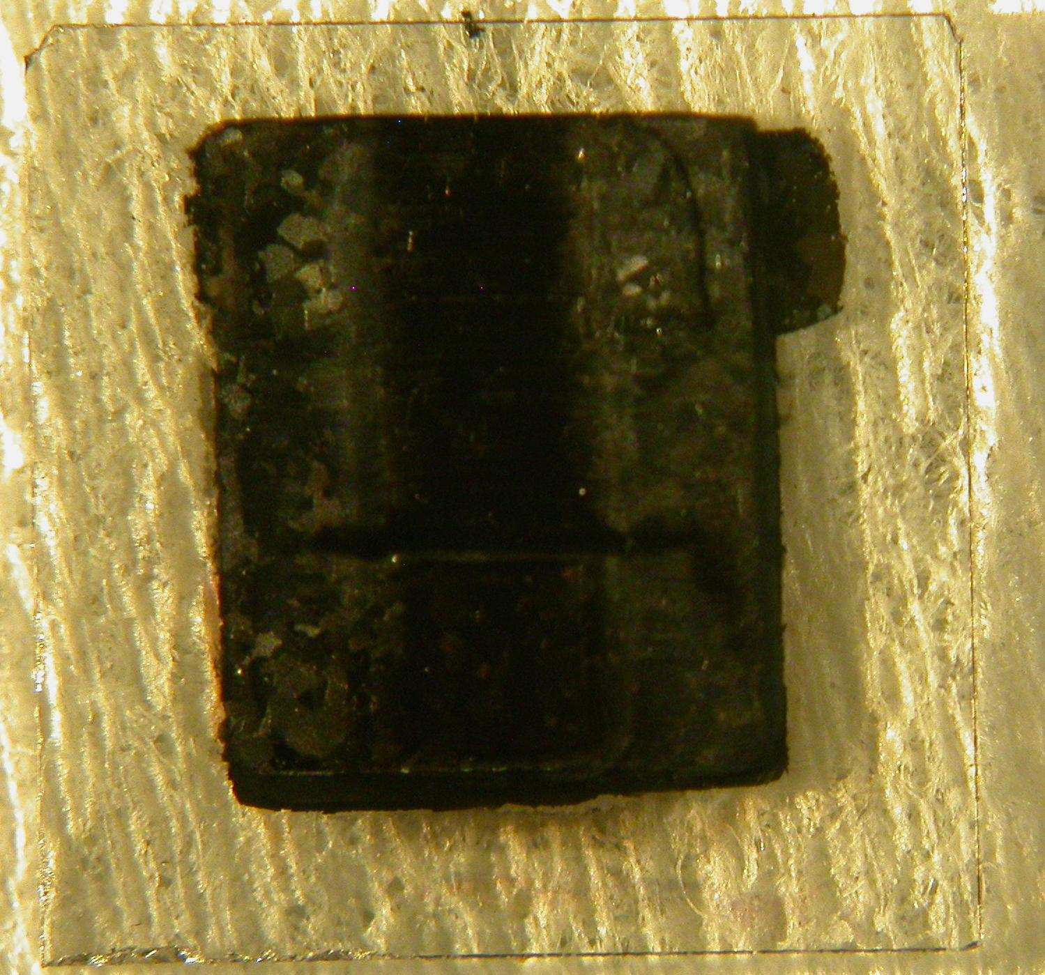
Figure 1.
Optical microscopy image of detector-grade poly-crystal CVD diamond with
dimensions 5x5x0.3 mm3
with photo-generated graphite electrical
contact made on the both sides.
The laser emitted 20 nsec long pulse with an energy of
about 160 mJ/pulse at 10 Hz repetition
rate. In order to focus the UV laser and reach therequired energy density
per pulse an appropriate UV focusing system was needed. The laser beam
with a transverse size of about 20
×10
mm2
,
was directed onto a homogenizer single matrix. The homogenized beam was
then directly projected via a thin and plain convex lens onto the sample.
The sample was placed in a holder and rigidly fixed to a
x-y movable stage. The x and y positions were controlled by two step
computer assisted motors.
The focused image was a square of 3 mm
2
at the sample surface and having a
local laser fluence of about 5 J/cm2
quite constant within the radiation
spot. The device was treated in air at room temperature and the surface
was scan at a velocity of about 0.3 mm/s to obtain a graphite electrode with a final total area of about 9 mm2 large enough to realize a pad detector.
This treatment was repeated on the other side of the surface sample (Figure 1) in order to realize
a solid state radiation detector in planar configuration. The device was fixed between two gold made clamps in order to apply the high voltage by
a SMA connector and enclosed in an aluminum box to electrically
shield it.
The reference device was a commercially available
poly-crystal diamond detector of the same size 5x5x0.3mm
3
and material quality but with DLC/Pt/Au electrical contacts
fabricated on both faces (planar configuration) with proprietary contact
technology. The detector was glued on a printed circuit board in one side
and the two electrodes wire bonded to a SMA connector and enclosed also in
an anodized aluminum box.
A low intensity
60Co
gamma-ray source was placed above the detectors at a distance of 1 cm in
air at room temperature. The front-side electrode was used as the signal
output and connected, through ORTEC charge sensitive preamplifier and
spectroscopy amplifier ( 100mV/fC total gain and 0.5
μs shaping-time ), to an
oscilloscope and waveforms were recorded by GPIB protocol.
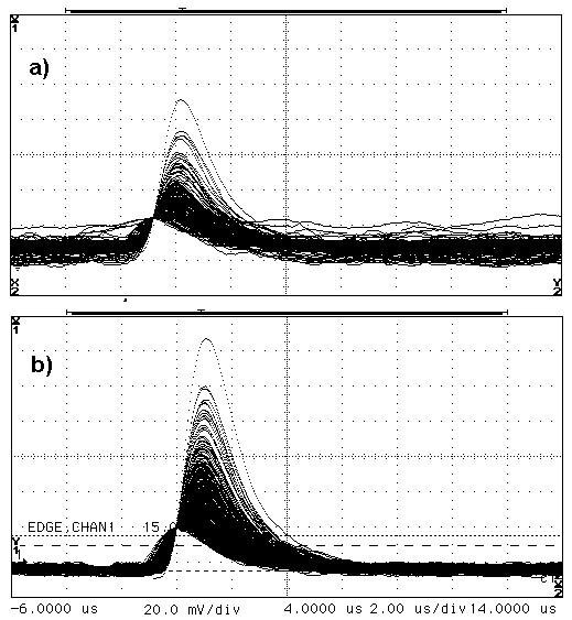
Figure 2. Single gamma response to
60Co
gamma source from reference diamond detector (waveforms a) and from
diamond detector with laser-graphitized electrodes (waveforms b) for an
applied voltage of about 300 V
Figure 2 shows the response of the two devices to gamma
radiations. The response is very similar showing that the nanographitic
layer is not a source of minority carriers trapping. This preliminary
result is very important to establish the good charge injection and
collection properties of the contacts, in addition to mechanical adhesion
and mechanical stability.