|
| |
|
P3HT and PCBM bilayer |
modified on
17/06/2012 |
-
-
The first single step MAPLE (ss-MAPLE) deposition of a
bilayer structure consisting of the most-studied donor-acceptor
combination for polymer solar cells, namely, the electron donating polymer
[regioregular polymer poly-(3-hexylthiophene) (P3HT) and the electron
accepting fullerene [6,6]-phenyl-C61-butyric-acid methylester (PCBM).
Furthermore, the same solvent has been used for both polymers, thus
overcoming the typical drawback of re-dissolution of the bottom layer
occurring in the conventional solution-based deposition techniques.
A polymeric solar cell based on the ss-MAPLE deposited
P3HT/PCBM heterojunction has been fabricated and characterized. The two
polymers, P3HT and PCBM (Sigma Aldrich), were both dissolved in toluene
with the weight concentration of 0.3 wt.%.
MAPLE depositions of each material were performed
using a pulsed Lambda Physik (LPX-305i) KrF excimer laser (l=248
nm, t=20 ns, pulse rate=10 Hz). To deposit P3HT and PCBM layers, 6000 and
4000 laser pulses were applied obtaining a corresponding final thickness
of 68 nm and 25 nm, respectively. UV-Vis absorption spectra were
acquired for the single polymer layers and for the bilayer structure,
deposited on silica slabs, using a Perkin Elmer spectrophotometer in the
wavelength range 350-750 nm with a resolution of 2 nm. Atomic force
microscopy (AFM), scanning electron microscopy (SEM), and energy
dispersive x-ray spectrometry (EDS) were used to characterize the
morphological and compositional properties of the deposited samples. In
particular, SEM and EDS analyses were performed by using a NVISION 40
Focussed Ion Beam (FIB) system equipped with a high resolution SEM Field
Emission Gun (FEG) Gemini column and an Inca Energy 350 X-ACT Oxford EDS
spectrometer.
Morphological and chemical investigations were carried
out both in plan view and cross-sectional geometry. AFM measurements were
performed in non contact mode (Park XE 70 instrument). Finally, a bilayer
solar cell was fabricated.
A
poly(3.4-ethylenedioxythiophene)-poly(styrenesulfonate) (PEDOT:PSS) layer
was spin-coated onto an ITO/glass substrate. Then, the active layer was
fabricated by depositing the bilayer structure onto the PEDOT:PSS layer
with 8000 laser pulses for P3HT layer (90 nm) and 4000 for PCBM layer (25
nm). To complete the device structure, LiF (0.6 nm-thick) and Al (ca.100
nm-thick) were thermally evaporated at low pressure (<1x10⁻⁶
Torr). The active area of the devices was 0.03 cm2).
Current density versus voltage (J-V) characteristics were measured using a
Keithley 2400 sourcemeter both in dark and under AM 1.5-G illumination,
filtered irradiation with an incident power of 100 mW/cm2).
All of the measurements were carried out under ambient conditions
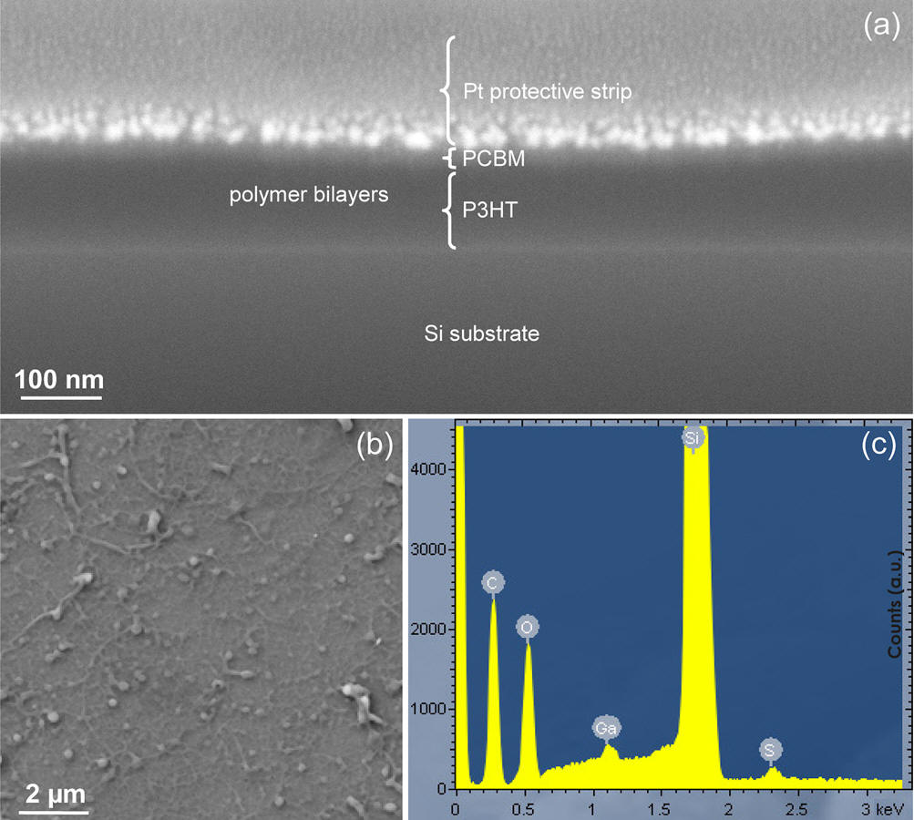
Figure 1.
Color online) Cross-section (a), top view (b), and
EDS spectrum (c) of the P3HT/PCBM bi-layer with a 68 nm thick layer of
P3HT and a 25 nm thick layer of PCBM
UV absorption spectra of the single layers of P3HT and
PCBM and of the bilayer P3HT/PCBM, are reported in Fig. 2., thus
excluding intermixing or damaging phenomena related to the bilayer
deposition. As a preliminary application, we tested the ss-MAPLE bilayer
production in fabricating a solar cell geometry based on the configuration
ITO/PEDOT:PSS/P3HT(90 nm)/PCBM(25 nm)/LiF/Al. The PEDOT:PSS was deposited
by spin-coating according to the standard procedure for the preparation of
conventional solar cells.
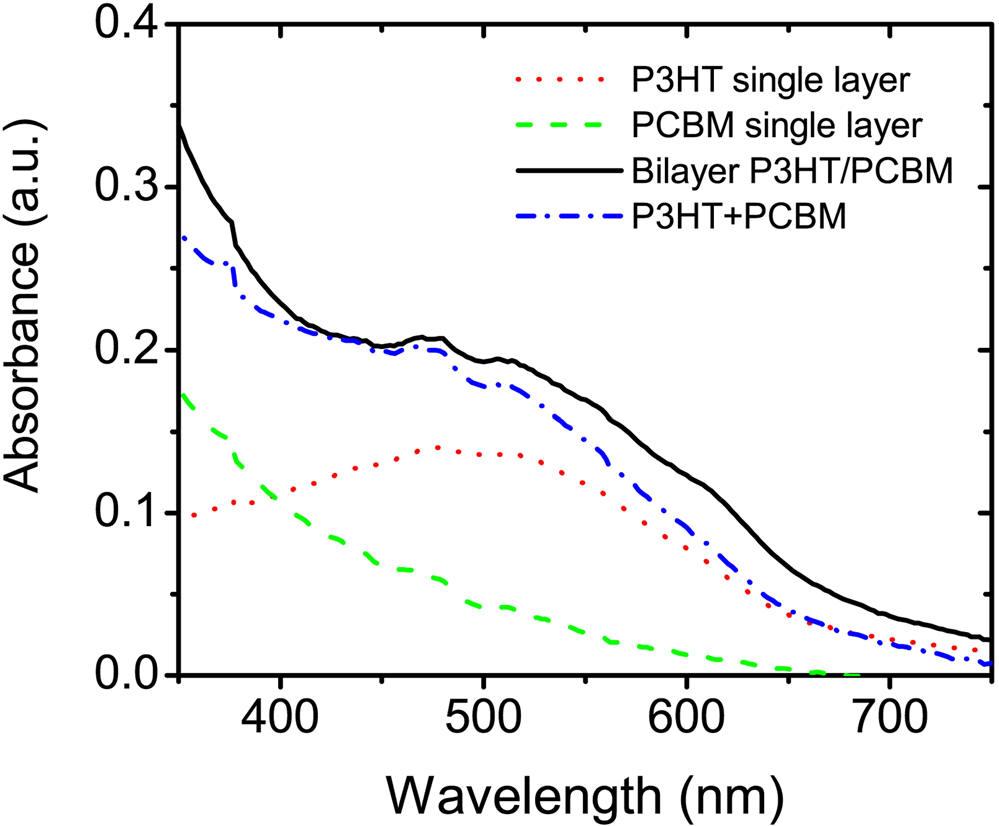
Figure 2. (Color online)
UV-visible absorption spectra of the P3HT single layer (dotted line), PCBM
single layer (dashed line), and P3HT/PCBM bilayer (full line). The
arithmetical sum of the absorption spectra of the two single layer
polymers is reportedtoo (dot-dashed line).
The layered structure of the device is sketched in Fig.
3, where it is shown the current density-voltage curves (dark and
illuminated) of the fabricated bilayer. The open circuit voltage is
Voc=0.32, the short circuit current is Jsc=0.33 mA/cm2),
the fill factor is FF=28%, and PCE=0.03%. Our ss-MAPLE deposition
procedure also rules out the contamination consequences related to the
MAPLE deposition experiments of organic bilayers, already reported in the
literature.
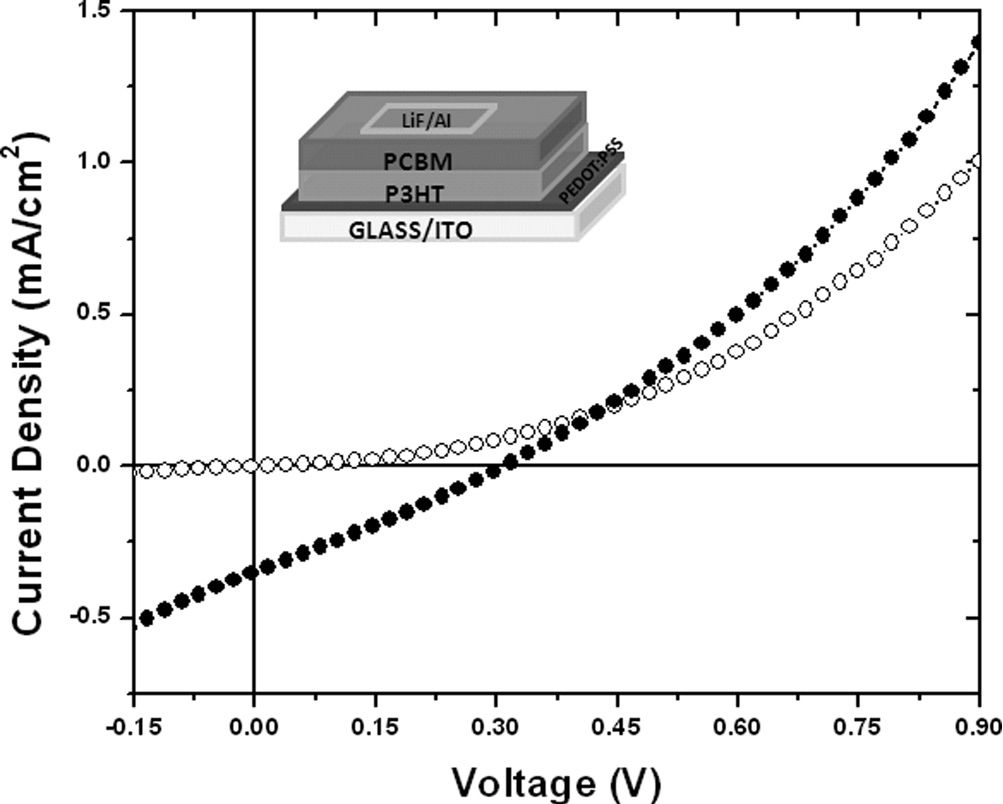
Figure 3. Current-voltage
characteristics of the bi-layer photovoltaic device in dark (open circles)
and under one-sun illumination (AM 1.5 G; filled circles). Inset image:
Sketch of the bilayer device structure fabricated by ss- MAPLE technique.
|
| |
|